Active Topics
  Memberlist
  Calendar
  Search
 | Active Topics Memberlist Calendar Search |
|
| |
 Topic: GATE-1999 Instrumentation Engg Topic: GATE-1999 Instrumentation Engg |
  |
| Author | Message |
|
Neha Agarwal
Groupie 
Joined: 04Jan2007 Online Status: Offline Posts: 59 |
  Topic: GATE-1999 Instrumentation Engg Topic: GATE-1999 Instrumentation EnggPosted: 05Jan2007 at 6:08pm |
|
1.1. (a) 0 (b) 1.1 (c) 0.5 (d) 1
1.2. For the waveform V (t) = 2 + cos (a) (c) p (d) 1.3. A system with transfer function (a) 6.9 s (b) 10 s (c) 14.4 s (d) 20 s
The transfer function of this system is (a) (b) (c) 1+ s 2e -2s
(d) 1+ s 2e 2s
1.5. A transfer function has two zeroes at infinity. Then the relation between the numerator degree (N) and the denominator degree (M) of the transfer function is, (a) N=M+2 (b) N=M-2 (c) N=M+1 (d) N=M-l
(a) 0.8 (c) -0.4 (b) 0.4 (d) unbounded
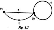
1.7. The transfer function betweenY 2 and Y 1 in Fig. 1.7 is
(a) a+b (b) (a+b)c (C) (d)
1.8. In control system design, gain and phase margins are usually provided to (a) account for the uncertainties in the system (b) make the system respond fast (c) reduce the overshoot in step response (d) reduce the steady state offset. 1.9. The lengths of two discrete time sequences X 1 (n) are 5 and 7 respectively. The maximum length of sequence x 1 (n) * x 2(n) is (a) 5 (b) 6 (c) 7 (d) 11
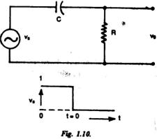
1.10. The output voltage of the circuit in Fig. 1.10 for t > 0 is
(b) (c) (d)
1.12. The input voltage, V 1 is 4 + 3 sin wt. assuming all elements to be ideal, the average of the output voltage V o in Fig. 1.12 is (a) -3 V (b) +3 V (c) -7 V (d) +7 V
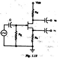
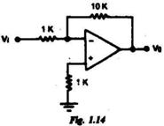
1.13. In the JFET amplifier circuit shown in Fig. 1.13, the signal outputs V 1 and v 2 are related as (a) (b) (c) (d) 1.14. The op-amp in the amplifier circuit shown in Fig. 1.14 has an offset voltage of 10 mV and it is ideal otherwise. If V i is zero, the output voltage V o is
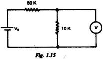
1.15. A voltmeter connected across the 10 k W resistor in the Fig. 1.15, reads 5 V. The voltmeter is rated at 1000 ohms/volt and has a full scale reading of 10 V. The supply voltage V s in volt is
|
|
|
For more papers visit:
http://onestopgate.com/gate-preparation// Post Resume: Click here to Upload your Resume & Apply for Jobs |
|
 IP Logged IP Logged |
|
| |
||
Forum Jump |
You cannot post new topics in this forum You cannot reply to topics in this forum You cannot delete your posts in this forum You cannot edit your posts in this forum You cannot create polls in this forum You cannot vote in polls in this forum |
|
|

© Vyom Technosoft Pvt. Ltd. All Rights Reserved.
 (a)
(a)  3V
3V 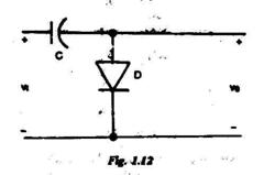
 0
0